Skip to content

Hardware

Notes from the PCBWay Assembly Floor: Header Pins, JST Footprints, and Switch Jumper Routing

Passing local Design Rule Checks (DRC) in KiCad is a satisfying milestone, but it is not the same thing as passing physical assembly on the factory floor.

Shortly after we submitted our initial 4-layer calculator mainboard (calculator.kicad_pcb), BOM (bom.csv), and pick-and-place centroid files to PCBWay for turnkey SMT and through-hole assembly, their engineering team paused the line and sent back a set of real bench inspection photos. Those photos caught four physical integration bugs that a software DRC never flags: through-hole MCU header pins colliding with a front-side tactile switch, a through-hole JST battery header paired with undrilled surface-mount pads, mirrored silkscreen layers, and implicit jumper connections across the 4-pad tactile switches.

Here is what the PCBWay team found on the bench and how we fixed the board layout and jumper routing with Python scripts in KiCad's pcbnew API.
The Postfix Manifesto: Why Human Thought Calculates in Stacks, Not Parentheses

For more than four decades, secondary and collegiate math education has been dominated by legacy in-fix computing architectures.

Generations of students have been handed monolithic graphing bricks, only to encounter endless parentheses soup, hidden order-of-operation syntax errors, and cryptic SYNTAX ERROR screen freezes. Today, that friction is compounded by recurring annual software emulator seat licenses, non-repairable assemblies, and battery corrosion.

StackCalc was born out of an uncompromising thesis: In-fix entry is a pedagogical bottleneck that hides mathematical truth inside a black box. The natural logic of human thought and physical reality is Postfix (Reverse Polish Notation).

The TPU Button Video Is a Design Review, Not a Slow-Motion Test

A simulation is much more useful when it makes a design argument visible. In a static CAD view, a TPU key, a faceplate opening, and a switch location can all look compatible. The difficult part happens between those still images: a keycap drops, tilts toward a wall, transfers motion through the web, and either reaches the switch or spends its travel rubbing somewhere it should not.

That is why we made a cutaway video of the StackCalc TPU membrane. It is a short design-review tool built from the same membrane and faceplate STL geometry used for the prototype, not a claim that the unpopulated calculator has already survived a life test. The RP2350 board is in fabrication; the video lets us inspect the mechanical questions now and gives the first board session specific cases to repeat.

We Pressed One TPU Key 280 Ways Before the PCB Arrived

A calculator key rarely gets pressed straight down in the middle. A thumb catches an edge. A finger comes in from the side. A child presses a corner. The first question for our TPU membrane was not “does it move?” It was “which bad presses leave enough room for the key to reach the switch without scraping the faceplate?”

The StackCalc PCB is in fabrication, so the printed calculator is not yet a powered keypad. We used the interval to put numbers around the geometry that will meet the board: the printed faceplate aperture, the TPU web, the keycap stem, and the proposed tactile-switch interface. That produced a 280-condition press sweep and the plot below.

What the First Printed StackCalc Prototype Can Teach Us

The first useful prototype is rarely the one that looks closest to a product. It is the one that makes the next decision cheaper. The current StackCalc hardware is a 3D-printed, tool-free mechanical prototype. Its KiCad PCB design is complete and fabrication is in progress, but there is no assembled, powered StackCalc board yet. The print lets us ask clearly: does the insertion path make sense, where does a part bind, and which keypad assumptions should be tested next?

From an Origami Box to a Puzzle Stand

Shipping support is usually dead weight: it protects a device for one trip and then disappears into a bin. We wanted the StackCalc packaging support to keep earning its space on a desk or shelf. That changed the design question from “how do we protect a calculator?” to “what can protect it, organize the kit, and become useful after unboxing?”

The first answer was an origami fold. The current answer is a printed puzzle stand: four dovetail-connected corner pieces form an upright shelf stand, while a separate strut becomes a low desktop typing support. The printed pieces and the package envelope are still being refined together, but the change already made the whole product feel more connected—from the first opened box to the way the calculator lives between uses.

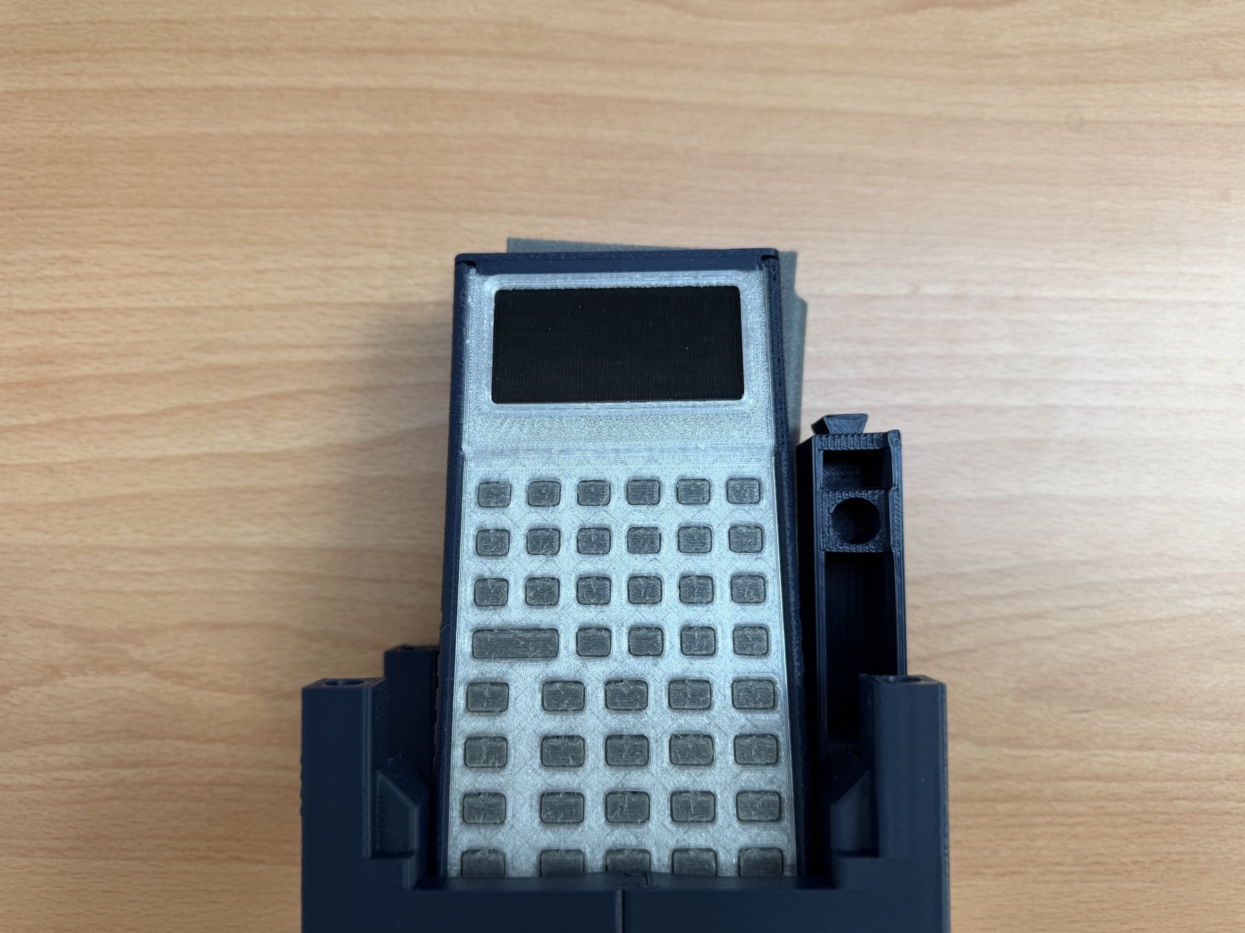
A printed StackCalc prototype docked in the shelf-stand assembly.

A Tool-Free Calculator Built Around a Sliding Assembly

“Tool-free” is easy to write on a feature list and hard to make useful in a printed enclosure. The test is not whether an assembly has no screws; it is whether a person can insert, retain, inspect, and later release the parts without turning every opening into a breakage risk.

The current StackCalc assembly is an unpowered, four-part mechanical prototype: a tapered chassis, unified faceplate, TPU membrane, and snap-retained top cap. Its RP2350 KiCad board is in fabrication, but no assembled board has been installed, so this remains a mechanical design lesson rather than an electronics assembly claim.

What the Firmware Simulator Can Tell Us Before Board Bring-Up

The current StackCalc prototype is a 3D-printed, tool-free mechanical assembly. Its RP2350 calculator PCB design is in fabrication, but no board has yet been assembled and powered, so we cannot yet make claims about powered bring-up, battery life, display behavior, or key feel on the finished electronics.

That is why the firmware simulator is useful. It gives us a fast way to exercise the calculator software and its proposed row-and-column interface while the physical electronics are still being developed. It is evidence about the simulated build, not evidence that a physical PCB works.