Notes from the PCBWay Assembly Floor: Header Pins, JST Footprints, and Switch Jumper Routing
Passing local Design Rule Checks (DRC) in KiCad is a satisfying milestone, but it is not the same thing as passing physical assembly on the factory floor.
Shortly after we submitted our initial 4-layer calculator mainboard (calculator.kicad_pcb), BOM (bom.csv), and pick-and-place centroid files to PCBWay for turnkey SMT and through-hole assembly, their engineering team paused the line and sent back a set of real bench inspection photos. Those photos caught four physical integration bugs that a software DRC never flags: through-hole MCU header pins colliding with a front-side tactile switch, a through-hole JST battery header paired with undrilled surface-mount pads, mirrored silkscreen layers, and implicit jumper connections across the 4-pad tactile switches.
Here is what the PCBWay team found on the bench and how we fixed the board layout and jumper routing with Python scripts in KiCad's pcbnew API.
1. The Red Box: Rear MCU1 Header Pins vs. Front Tactile Switch SOFT6
In our prototype architecture, the Raspberry Pi Pico 2 (MCU1) mounts horizontally on the back of the mainboard (B.Cu), while the 43 tactile switches (B1–B37 and SOFT1–SOFT6) mount on the front (F.Cu).
In our initial BOM, we accidentally specified part number SC1632 (the Raspberry Pi Pico 2 with pre-soldered through-hole header pins) alongside a plated through-hole (PTH) footprint in KiCad. When PCBWay's technicians dry-fitted the module from the rear, the header pins poked straight through the \(1.6\text{ mm}\) FR-4 substrate and emerged on the front face—right inside the courtyard of softkey SOFT6:
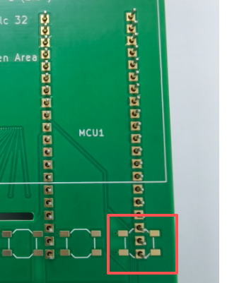 Figure 1: PCBWay bench inspection photo (
headers.png). The red box highlights the rear MCU1 through-hole header pins poking through the front of the board directly between the four SMD pads of tactile switch SOFT6.
Even if those protruding pins were clipped flush after soldering, the exposed solder fillets and pin tips sat directly beneath the metal snap-dome body of SOFT6, preventing the switch from seating flat on its F.Cu pads and risking a dead short against the switch housing.
The Fix: Castellated SMD Mounting (SC1631) & fix_mcu_pads.py
Because the Raspberry Pi Pico 2 features castellated edge pads along all 40 pins, through-hole headers are completely unnecessary when mounting the module flush against the rear copper layer. We:
1. Updated MCU1 in bom.csv from SC1632 (pre-headered) to SC1631 (bare castellated Pico 2).
2. Wrote a pcbnew script (Hardware/fix_mcu_pads.py) to convert all 40 MCU1 pads from PAD_ATTRIB_PTH to pure bottom-side PAD_ATTRIB_SMD (B.Cu, B.Paste, B.Mask) with zero drill holes, leaving the front switch surface unbroken.
2. The JST1 Footprint Mismatch & Stranded Front Silkscreen
The second photo from PCBWay flagged JST1, our 2-pin right-angle battery connector at the top-right corner of the board:
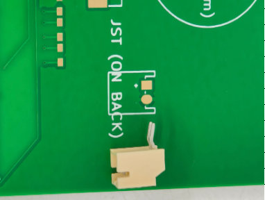 Figure 2: PCBWay bench photo (
jst.png) showing the through-hole S2B-PH-K-S header next to the surface-mount JST1 pads.
Two things had gone wrong simultaneously:
1. Through-Hole Part vs. SMD Pads: Our BOM listed S2B-PH-K-S(LF)(SN)—a through-hole right-angle JST PH header with bent metal pins—while the footprint on the board used undrilled surface-mount pads. We updated bom.csv to specify the surface-mount S2B-PH-SM4-TB right-angle connector (and coordinated the jumper/lead seating for the initial boards with the PCBWay assembly team).
2. Mirrored Silkscreen on the Wrong Layer: Notice how the text JST (ON BACK) in Figure 2 and the MCU1 outline in Figure 3 below were printed in white silkscreen on the front (F.Silkscreen) of the green board, even though both components mount on the back!
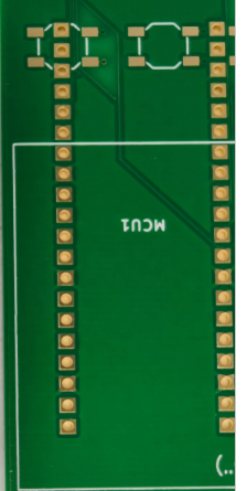 Figure 3: PCBWay bench photo (
silkscreen.png) showing MCU1 silkscreen graphics stranded on F.Silkscreen and overlapping the upper switch row.
When we originally flipped MCU1 to the back layer in KiCad, several child graphical primitives inside the footprint remained explicitly bound to F.Silkscreen and F.Fab. We wrote Hardware/fix_silkscreen.py to iterate through every graphical item and standalone text callout, migrating them to B.Silkscreen and B.Fab with proper mirroring.
3. Cleaning Up Tactile Switch Jumper Connections
The most subtle issue involved how the 43 tactile switches (SW_TACT_ALPS_SKQGABE010) were wired into the \(8 \times 6\) keypad matrix.
A standard 4-terminal SMD tactile switch has two internally bridged pairs of legs (legs 1–1' form one continuous metal bar inside the switch body, and legs 2–2' form the switched bar). Many community KiCad footprints assign duplicate pad numbers (1, 1 and 2, 2) with (duplicate_pad_numbers_are_jumpers yes), allowing the router to pass a row or column bus through the switch's internal metal frame instead of routing a continuous copper trace on the PCB.
During DFM review and rework around the MCU1 / SOFT6 overlap zone, relying on implicit switch-body jumpers and ambiguous 4-pad assignments created confusion about which pads required active electrical jumpering versus mechanical anchoring:
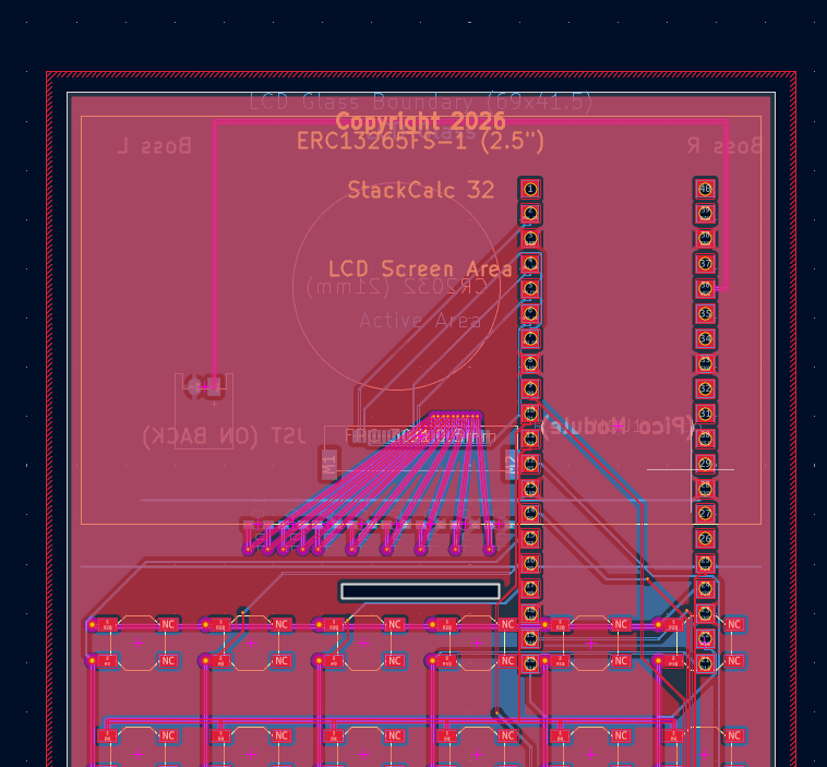 Figure 4: Updated KiCad layout (
kicad.png) with (duplicate_pad_numbers_are_jumpers no), explicit active pads (1 and 2), isolated NC anchor pads, and continuous copper bus routing.
To make the schematic-to-board netlist 100% explicit for both the pick-and-place line and our rework instructions:
* We set (duplicate_pad_numbers_are_jumpers no) across every tactile switch footprint on the board.
* We designated the left-side pair as active electrical pads 1 (row net) and 2 (column net), and explicitly marked the opposite mechanical stabilizing pads as NC.
* We rerouted the row and column buses (P0–P21) as continuous \(0.25\text{ mm}\) copper segments on F.Cu and B.Cu, eliminating any dependency on internal switch jumpers to carry matrix continuity downstream.
4. Exporting dummy_pcb.stl from pcbnew for 3D-Printed Enclosure Test-Fitting
While resolving the electronic DFM items with PCBWay, we also needed to verify that our 4-part screwless sliding enclosure (chassis, unified_faceplate, tpu_membrane, and snap-fit top_cap) had zero mechanical interferences with the populated board.
Rather than waiting for physical fiberglass boards to arrive to test our \(0.40\text{ mm}\) lateral PCB rail clearances and \(0.10\text{ mm}\) switch plunger datum, we wrote Hardware/generate_scad.py using KiCad's Python API (pcbnew). Every time make layout runs, it inspects calculator.kicad_pcb and generates two OpenSCAD files:
1. pcb_layout_generated.scad: Extracts the exact \((X, Y)\) centers of all 43 tactile switches, the internal Edge.Cuts LCD FPC ribbon slot, and the rear component sweeps.
2. dummy_pcb.scad \(\rightarrow\) dummy_pcb.stl: A complete 3D-printable plastic replica of the populated PCB—including the \(1.6\text{ mm}\) FR-4 substrate, all 43 switch bodies and actuator stems, the rear MCU1 Pico 2 envelope, the J1 0.5mm ZIF socket, JST1, and the C1–C8 charge-pump capacitors.
By printing dummy_pcb.stl in PLA on our desktop printer, we slid the populated plastic "board" into the chassis rails, verified that all 43 Shore 95A TPU membrane plungers met the switch tops cleanly, and confirmed battery lead clearances before PCBWay finished final assembly.