How the PCB Design Shapes a Printed Calculator Before It Arrives
The printed StackCalc enclosure is not a generic case waiting for an electronics design. Its CAD reads fixed coordinates from the KiCad board so the rails, display opening, key interfaces, and clearances are designed around the same board that is now in fabrication.
One board, several design decisions
The active KiCad project is Hardware/calculator.kicad_pcb. The hardware generator extracts the board’s fixed coordinates before producing the chassis, faceplate, TPU membrane, and top-cap exports. That keeps a change to a switch or display interface visible as a mechanical consequence instead of allowing a rendered enclosure and a PCB to drift apart.
The manufacturing BOM records the chosen RP2350/Pico 2 controller, ERC13265FS 132 × 65 LCD, 0.5 mm-pitch FPC display connector, ALPS tactile switches, JST battery connector, and display-support passives. These are selected and sourced manufacturing components, not props added after the enclosure was drawn.
Why this matters before bring-up
The same board definition guides the firmware simulator’s 132 × 65 display buffer and row-and-column keypad contract. It also constrains physical placement: the faceplate aperture must clear the display interface, the flexible membrane has to meet the intended switch locations, and the enclosure needs a service path that does not pinch the board or wiring.
The current printable assembly lets us inspect that geometry, while the emulator lets us test the logical paths that will use it. Neither substitutes for board bring-up. Once the fabricated board is populated, we will validate electrical connections, display initialization, power use, key travel, and the fit of the actual component stack against the same revision.
Treat the board outline as a mechanical datum
The enclosure began from a board-aware coordinate system rather than an empty rectangle. Once the KiCad layout fixes a display window, connector direction, switch layer, controller position, battery clearance, and mounting keep-outs, each of those positions becomes a constraint for the printed chassis. A wall moves because a connector needs service space; a key support moves because it has to meet the switch layer below the membrane.
That makes the first board arrival a focused fit session. We will check the board seating plane, display alignment within the faceplate opening, flex and connector clearance, matrix reach under the membrane, and whether the cap closes without touching an electronic component. Those checks are easier to reason about because both the board and the mechanical prototype have already been developed from the same envelope.
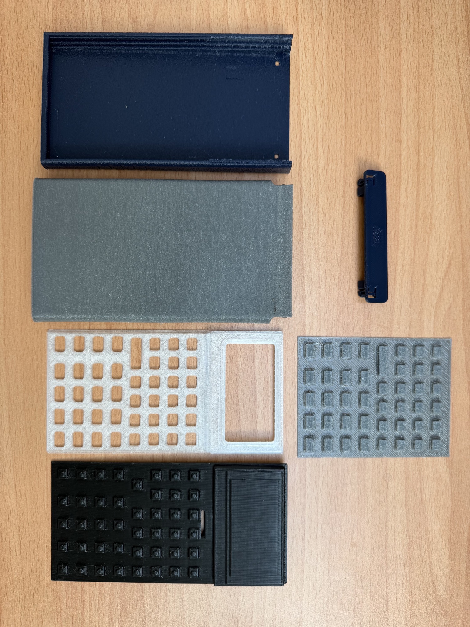
The project publishes printable mechanical and teacher materials, not the private electronics source. The hardware guide describes the current kit, while the firmware simulator post shows how the software path is exercised before board bring-up. That leaves a clear handoff: the board is already designed and in fabrication; the next evidence is physical integration, not a redesign invented after delivery.
Use a checklist when the board arrives
The first fit should be photographed and recorded against the same CAD revision used for the print: board seats flat, every connector has its intended approach path, the display sits centred in the opening, membrane features reach their switch positions, and the cap closes without a hidden collision. That is a modest checklist, but it turns a delivery-day surprise into a change list that crosses the electrical and mechanical models cleanly. The project will publish the resulting physical fit observations with the next hardware log.